Quantum technologies
What are quantum technologies?
These are technologies that aim to exploit quantum mechanical phenomena for some useful application. Quantum computing is a very important quantum technology, where the building blocks are quantum bits or qubits, see https://youtu.be/g_IaVepNDT4
Another is quantum communication, which can, in theory, deliver a completely secure communication channel. The European quantum communication infrastructure will be based on fibre optics using 1.5 µm light https://youtu.be/sheIkirO778
What quantum technologies are we focussing on at Salford?
Here we are focussing on technologies based on erbium-implanted silicon devices.
Why silicon?
The best material and device structure required for a high-performance quantum computer is hotly debated, but some of the most promising schemes for large scale quantum computes require devices with sizes on the order of a few atoms. Silicon is by far the best material to fabricate devices of this scale. The dimensions of transistors in silicon microprocessors can currently be made as small as 2 nm (about 20 atoms), see below.
Why erbium?
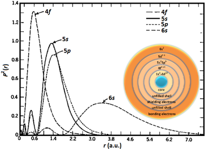
In the rare earth elements, including erbium, optical and microwave (spin) transitions occur in the 4f-orbital. The f-orbital is located close to the nucleus, while other orbitals lie further out, see below. These outer orbitals shield the f-orbital from effects that can lead to the breakdown of delicate quantum states, known as decoherence. Resistance to decoherence is an important property for qubits.
Erbium is notable among the rare earth elements because the main 1.5 µm wavelength of light it gives off matches almost exactly the lowest loss wavelength of the optical fibre used in internet communication. The light signals in optical fibre need to be amplified every 100 km or so. This can be done using a section of fibre doped with erbium in what is known as an erbium doped fibre amplifier (EDFA). Today’s high bandwidth internet services would not function without the EDFA.
Why ion implantation?
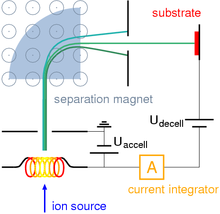
Ion implantation is the method of choice for intruducing impurities into silicon required for the transistors in microprocesors to function. The schematic of an ion implanter is shown below. Here a material containing the desired element for implantation is vaporised then accelerated with a high voltage, the desired ions are then separated with a large magnet, which can actualy sepatate out the different isotopes of a particular ion. The ions are then fired at the target material substrate. The speed (and therefor depth of penetration), position on the substrate surface, and flow rate of ions can be precisley cotrolled.
Using silicon processing and ion implantation will make building large scale quantum devices and systems more practical than using other technologies.
Spin echo measurements
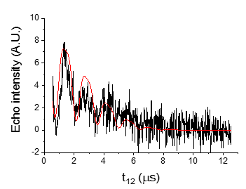
A sequence of microwave pulses can produce an echo as long as the erbium spin is in a superposition of states. We measured the spin coherence time of Er implanted Si to be 7.5 μs, which was the first measurement of the spin coherence time of any implanted rare earth [1].
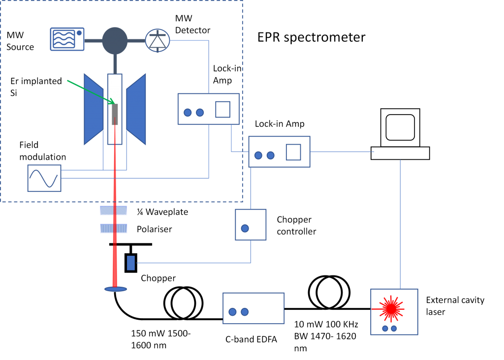
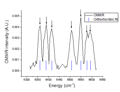
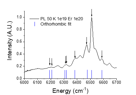
Optically modulated magnetic resonance (OMMR)
OMMR is a technique developed by Dr Mark Hughes at Salford university to understand the various optical and magnetic centres in Er:Si [2].
OMMR was used to make the first measurement of the crystal field splitting of the first excited state of Er implanted Si.
The OMMR mechanism involves excitation from the Si valence band to the first excited states of Er by tuneable 1.5 µm laser light. This excitation relaxes to the Er Zeeman ground state via an intermediate Er defect state. Population of the Er Zeeman ground state reduces saturation of the Zeeman transition and results in an increase in microwave absorption, which increases the EPR signal.
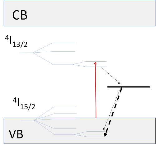
The OMMR spectrum of Er implanted Si can be fitted to a set of orthorhombic crystal field parameters which predict peaks in the photoluminescence spectrum of Er implanted Si, and vice versa.
Superconducting resonator coupling
Er implanted Si can be coupled to a superconducting resonator. An Er implanted Si sample was placed face-on to an NbN lumped-element micro-resonator on Al2O3 at 20 mK.
The micro-resonator Q-factor was measured as a function of magnetic field and orientation to give an effective orientation dependent EPR measurement using a micro-resonator [3].
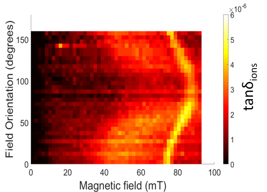
There was a good correspondence with modelling using previously measured EPR parameters for Er-implanted Si and represents the first coupling of Er implanted Si to a superconducting resonator.
Please contact Dr. Mark Hughes if you are interested in working with us or conducting postgraduate research on this topic.
References
1. Hughes, M.A., et al., Spin echo from erbium implanted silicon. Applied Physics Letters, 2021. 118: p. 194001 https://doi.org/10.1063/5.0046904
2. Hughes, M.A., et al., Optically modulated magnetic resonance of erbium implanted silicon. Scientific Reports, 2019. 9(1): p. 19031. https://doi.org/10.1038/s41598-019-55246-z
3. Hughes, M.A., et al., Coupling of Erbium-Implanted Silicon to a Superconducting Resonator. Physical Review Applied, 2021. 16(3): p. 034006.